- 您现在的位置:买卖IC网 > Sheet目录337 > LH28F320SKTD-ZR (Sharp Microelectronics)IC FLASH 32MBIT 70NS 48TSOP
�� �
�
�LHF32KZR�
�3�
�Internal� V� CC� and� V� PP�
�1� INTRODUCTION�
�This� datasheet� contains� LH28F320SKTD-ZR�
�specifications.� Section� 1� provides� a� flash� memory�
�overview.� Sections� 2,� 3,� 4,� and� 5� describe� the�
�memory� organization� and� functionality.� Section� 6�
�covers� electrical� specifications.�
�1.1� Product� Overview�
�The� LH28F320SKTD-ZR� is� a� high-performance� 32M-�
�bit� Smart3/5� Dual� Work� Flash� memory� organized� as�
�2MBx8/1MBx16� x� 2Bnak.� The� 4MB� of� data� is�
�arranged� in� sixty-four� 64K-byte� blocks� which� are�
�individually� erasable,� lockable,� and� unlockable� in-�
�system.� The� memory� map� is� shown� in� Figure� 3.�
�Smart3/5� technology� provides� a� choice� of� V� CC� and�
�V� PP� combinations,� as� shown� in� Table� 1,� to� meet�
�system� performance� and� power� expectations.� 2.7V�
�V� CC� consumes� approximately� one-fifth� the� power� of�
�5V� V� CC� .� But,� 5V� V� CC� provides� the� highest� read�
�performance.� V� PP� at� 2.7V,� 3.3V� and� 5V� eliminates�
�the� need� for� a� separate� 12V� converter,� while� V� PP� =5V�
�maximizes� erase� and� write� performance.� In� addition�
�to� flexible� erase� and� program� voltages,� the� dedicated�
�V� PP� pin� gives� complete� data� protection� when�
�V� PP� ≤� V� PPLK� .�
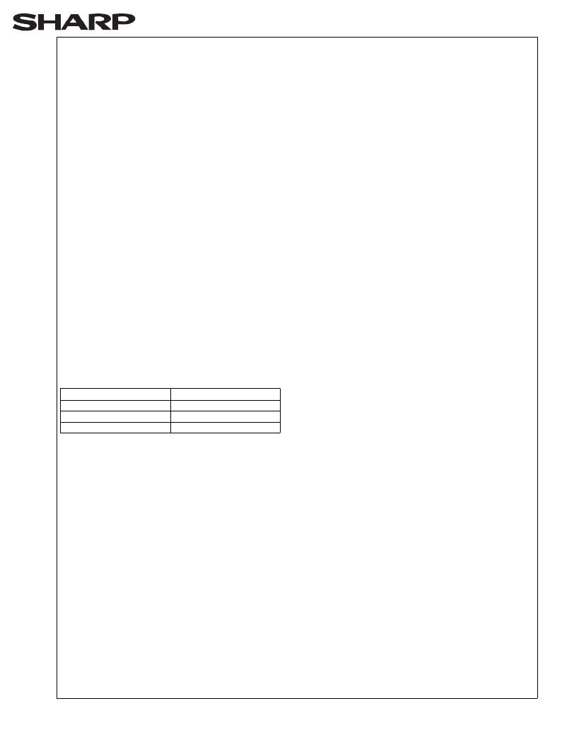
�Table� 1.� V� CC� and� V� PP� Voltage� Combinations�
�Offered� by� Smart3/5� Technology�
�V� CC� Voltage� V� PP� Voltage�
�2.7V� 2.7V,� 3.3V,� 5V�
�3.3V� 3.3V,� 5V�
�5V� 5V�
�detection� Circuitry�
�automatically� configures� the� device� for� optimized�
�read� and� write� operations.�
�A� Command� User� Interface� (CUI)� serves� as� the�
�interface� between� the� system� processor� and� internal�
�operation� of� the� device.� A� valid� command� sequence�
�written� to� the� CUI� initiates� device� automation.� An�
�internal� Write� State� Machine� (WSM)� automatically�
�executes� the� algorithms� and� timings� necessary� for�
�block� erase,� bank� erase,� (multi)� word/byte� write� and�
�block� lock-bit� configuration� operations.�
�A� block� erase� operation� erases� one� of� the� device’s�
�64K-byte� blocks� typically� within� 0.34s� (5V� V� CC� ,� 5V�
�V� PP� )� independent� of� other� blocks.� Each� block� can� be�
�independently� erased� 100,000� times� (3.2� million�
�block� erases� per� bank).� Block� erase� suspend� mode�
�allows� system� software� to� suspend� block� erase� to�
�read� or� write� data� from� any� other� block.�
�A� word/byte� write� is� performed� in� byte� increments�
�typically� within� 9.24μs� (5V� V� CC� ,� 5V� V� PP� ).� A� multi�
�word/byte� write� has� high� speed� write� performance� of�
�2μs/byte� (5V� V� CC� ,� 5V� V� PP� ).� (Multi)� Word/byte� write�
�suspend� mode� enables� the� system� to� read� data� or�
�execute� code� from� any� other� flash� memory� array�
�location.�
�Individual� block� locking� uses� a� combination� of� bits�
�and� WP#,� Sixty-four� block� lock-bits,� to� lock� and�
�unlock� blocks.� Block� lock-bits� gate� block� erase,� bank�
�erase� and� (multi)� word/byte� write� operations.� Block�
�lock-bit� configuration� operations� (Set� Block� Lock-Bit�
�and� Clear� Block� Lock-Bits� commands)� set� and�
�cleared� block� lock-bits.�
�The� status� register� indicates� when� the� WSM’s� block�
�erase,� bank� erase,� (multi)� word/byte� write� or� block�
�lock-bit� configuration� operation� is� finished.�
�The� STS� output� gives� an� additional� indicator� of� WSM�
�activity� by� providing� both� a� hardware� signal� of� status�
�(versus� software� polling)� and� status� masking�
�(interrupt� masking� for� background� block� erase,� for�
�example).� Status� polling� using� STS� minimizes� both�
�CPU� overhead� and� system� power� consumption.� STS�
�pin� can� be� configured� to� different� states� using� the�
�Configuration� command.� The� STS� pin� defaults� to�
�RY/BY#� operation.� When� low,� STS� indicates� that� the�
�WSM� is� performing� a� block� erase,� bank� erase,� (multi)�
�word/byte� write� or� block� lock-bit� configuration.� STS-�
�High� Z� indicates� that� the� WSM� is� ready� for� a� new�
�command,� block� erase� is� suspended� and� (multi)�
�word/byte� write� are� inactive,� (multi)� word/byte� write�
�are� suspended,� or� the� device� is� in� deep� power-down�
�mode.� The� other� 3� alternate� configurations� are� all�
�pulse� mode� for� use� as� a� system� interrupt.�
�发布紧急采购,3分钟左右您将得到回复。
相关PDF资料
LHF00L28
IC FLASH 16MBIT 70NS 48TSOP
LPM409 CHASSIS
STNRD 4SLOT CHASSIS W/INPUT LEAD
LS15RB1201J04
POE SPLITTER 10.8W 12V @0.9A
LT1932ES6#TRMPBF
IC LED DRIVR WHITE BCKLGT TSOT-6
LT1937ES5#TRMPBF
IC LED DRIVR WHITE BCKLGT TSOT-5
LT3003EMSE#TRPBF
IC LED DRIVER BALLASTER 10-MSOP
LT3465AES6#TRMPBF
IC LED DRIVR WHITE BCKLGT TSOT-6
LT3466EDD-1#PBF
IC LED DRIVR WHITE BCKLGT 10-DFN
相关代理商/技术参数
LH28F400BG
制造商:SHARP 制造商全称:Sharp Electrionic Components 功能描述:4M-BIT(256KBx16) SmartVoltage Flash MEMORY
LH28F400BGB-BL12
制造商:未知厂家 制造商全称:未知厂家 功能描述:x16 Flash EEPROM
LH28F400BGB-BL85
制造商:未知厂家 制造商全称:未知厂家 功能描述:x16 Flash EEPROM
LH28F400BGB-TL12
制造商:未知厂家 制造商全称:未知厂家 功能描述:x16 Flash EEPROM
LH28F400BGB-TL85
制造商:未知厂家 制造商全称:未知厂家 功能描述:x16 Flash EEPROM
LH28F400BGE-BL12
制造商:未知厂家 制造商全称:未知厂家 功能描述:x16 Flash EEPROM
LH28F400BGE-BL85
制造商:未知厂家 制造商全称:未知厂家 功能描述:x16 Flash EEPROM
LH28F400BGE-TL12
制造商:未知厂家 制造商全称:未知厂家 功能描述:x16 Flash EEPROM